/dqc/media/agency_attachments/2026/08/21/2026-08-21t061716244z-dq-channels-logojpg-2026-08-21-11-47-17.jpeg)

/dqc/media/media_files/2026/09/10/dq-channels-whatsapp-2026-09-10-17-07-48.png)

 Follow Us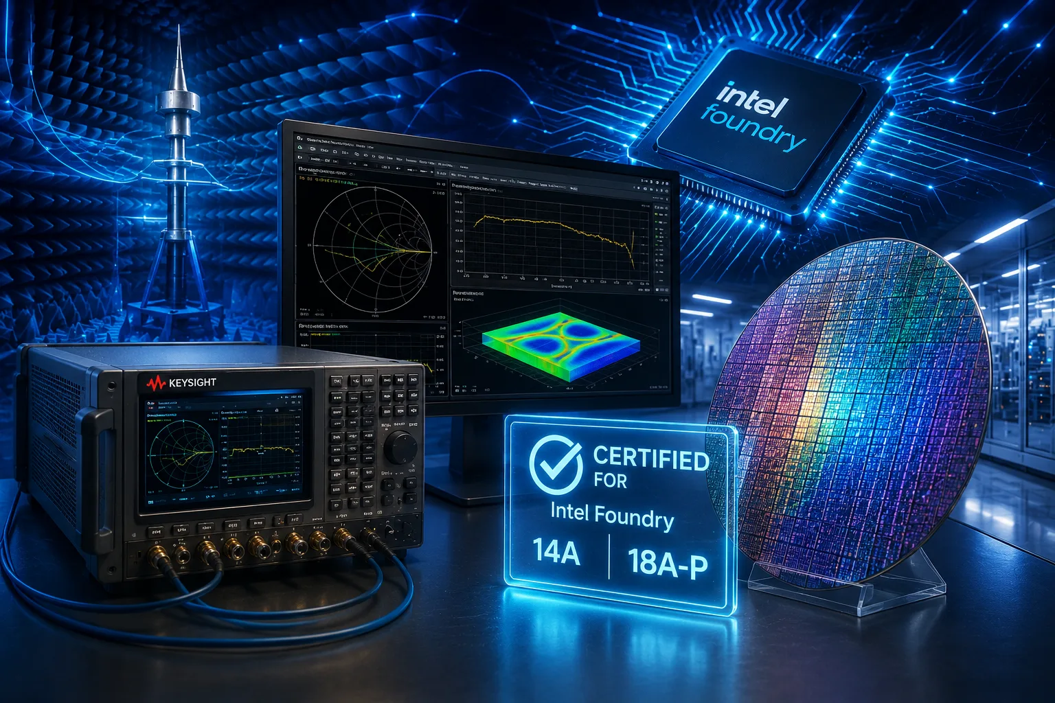
Keysight Technologies has announced the official certification of its RFPro electromagnetic (EM) design software, a key component of the Keysight EDA Advanced Design System (ADS), for Intel Foundry’s Intel 14A and Intel 18A-Pprocess technologies.
The certification provides radio frequency integrated circuit (RFIC) and mixed-signal design engineers with validated, production-ready simulation tools. This ensures that high-frequency electromagnetic models accurately reflect physical silicon behaviour prior to tape-out and commercial fabrication.
As semiconductor manufacturers push fabrication boundaries beyond sub-2nm thresholds, design complexity rises exponentially. Parasitic coupling, substrate loss, and complex interconnect cross-talk can cause significant mismatches between predicted circuit behaviour and post-fabrication performance.
If these electromagnetic discrepancies surface only after tape-out, engineering teams face multi-million-dollar chip re-spins and months of delayed product launches. Keysight’s pre-silicon certification establishes a verified design flow that reduces financial risk and accelerates time-to-market.
Supporting Next-Generation Transistor and Power Architectures
The certification validates Keysight RFPro against Intel Foundry’s evolving technology roadmap as customers transition from baseline Intel 18A to performance-enhanced Intel 18A-P, and onward to Intel 14A. The Intel 14A process node introduces two architectural shifts:
RibbonFET 2 Transistors: Intel's second-generation Gate-All-Around (GAA) architecture, delivering improved drive current and channel control at ultra-scaled dimensions.
PowerDirect Technology: An advanced backside power delivery network (BSPDN) that decouples power routing from signal interconnect layers, significantly reducing IR drop and optimising metal layer efficiency.
Extracting electromagnetic behaviour across these 3D transistor geometries and backside power grids requires high-precision EM solvers. RFPro seamlessly handles these complex 3D structures directly within the Keysight ADS layout environment. This enables designers to run interactive EM extraction without tedious manual layout preparation.
Sustained Ecosystem Collaboration Across Packaging Generations
This milestone extends an ongoing technology alliance between Keysight and Intel Foundry. Keysight previously delivered validated EDA workflows for Intel 18A as well as EMIB-T (Embedded Multi-die Interconnect Bridge with Through-Silicon Vias) advanced packaging technology.
By unifying EM simulation across both single-chip process nodes and multi-die heterogeneous packaging, Keysight provides a consistent design methodology across product generations. This ecosystem support is critical for high-growth sectors, including:
Artificial Intelligence (AI) Accelerators: High-speed die-to-die interfaces requiring low-loss electromagnetic channels.
High-Performance Computing (HPC): Ultra-dense power delivery networks and wide-bus interconnects.
Mobile & Wireless Infrastructure: Next-generation 5G-Advanced and 6G RF transceivers operating at millimetre-wave frequencies.
| EDA & Node Parameter | Legacy Process Simulation | Keysight RFPro Certified Flow (Intel 14A / 18A-P) |
| Electromagnetic Validation | Post-layout static checks subject to empirical errors. | Pre-Silicon 3D Full-Wave Extraction: Direct PDK alignment. |
| Transistor Architecture Support | FinFET and standard planar structures. | RibbonFET 2 GAA: Precise modelling of multi-ribbon GAA channels. |
| Power Grid Extraction | Front-side routing parasitic estimates. | PowerDirect BSPDN: Full EM extraction of backside power networks. |
| Heterogeneous Integration | Single-die isolated simulation models. | EMIB-T Packaging Support: Multi-die interposer & bridge EM modelling. |
Shawn Han, Senior Vice President and General Manager, Foundry Services, Intel Corporation, emphasised the role of predictable execution in accelerating customer innovation:
“As our customers look to address next-generation demands through differentiated solutions, Intel Foundry believes predictable execution on our advanced process and packaging technologies will accelerate their innovation. By collaborating closely with ecosystem partners such as Keysight to certify world-class solutions, we are providing our customers with greater confidence they can achieve their power, performance and efficiency goals and get to market more quickly.”
Niels Faché, Senior Vice President, Keysight Design Engineering Software, highlighted the necessity of early tool adoption:
“Design teams can’t wait for a new process node to mature before they trust their simulation results. This certification means engineers can adopt Intel Foundry’s newest technologies early and get the silicon right the first time.”
By pairing certified EDA software with Intel Foundry's bleeding-edge fabrication capabilities, Keysight enables global semiconductor teams to push the limits of power, performance, and area (PPA), ensuring complex RFIC and mixed-signal designs achieve first-pass silicon success.
Read More:
Why AI-ready data centres need more than computing power
Why Dell believes AI PCs need consultative selling, not hardware transactions
Nutanix explains how hybrid multi-cloud services will define channel growth
From ERP to ERX: How AI Is Turning Planning into Intelligent Execution