/dqc/media/agency_attachments/2026/08/21/2026-08-21t061716244z-dq-channels-logojpg-2026-08-21-11-47-17.jpeg)

/dqc/media/media_files/2026/09/10/dq-channels-whatsapp-2026-09-10-17-07-48.png)

 Follow Us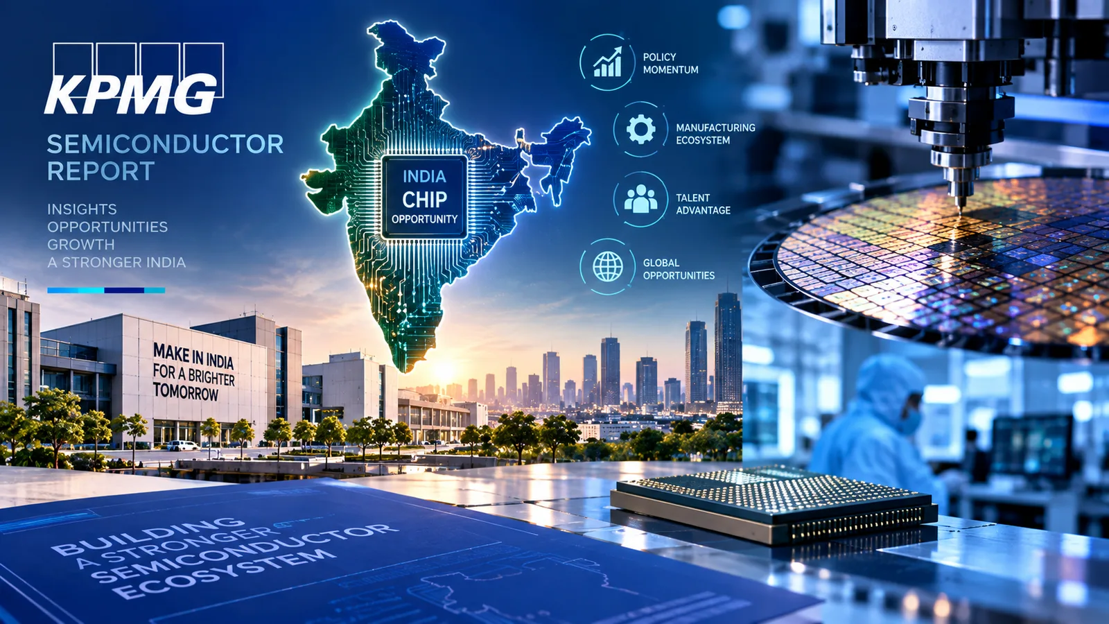
India’s semiconductor opportunity is moving beyond the question of whether the country can manufacture chips. The bigger challenge is building the capabilities around them. The KPMG semiconductor report, unveiled at SEMICON India 2026, looks at how policy support, domestic demand, engineering talent and emerging manufacturing capabilities could help build a globally competitive ecosystem.
The report projects India semiconductor demand to rise from around USD 44 billion in 2025-26 to nearly USD 90 billion by 2029-30. Mobile and wearables are expected to remain the largest segment, with demand estimated at about USD 42.13 billion.
India’s chip opportunity stretches beyond fabrication
The report takes an ecosystem-wide view of the India semiconductor market, covering design, manufacturing, advanced packaging, equipment, materials, R&D, talent, supply chains and technology commercialisation.
That broader approach is important because the report identifies indigenous intellectual property creation and commercialisation as a key part of the opportunity. For India, the goal is not limited to adding manufacturing capacity but also developing capabilities that can create value across the semiconductor chain.
Advanced packaging emerges as a key gap
The patent landscape offers a mixed picture. Between the decade ending June 2026, India recorded around 78,000 published semiconductor patent applications and approximately 28,000 grants. Semiconductor accelerators accounted for about 92% of filings within the technology categories tracked.
However, advanced packaging, high-bandwidth memory and chiplets remain comparatively thin areas. The report points to packaging as one area where India can build capability without the capital intensity associated with leading-edge wafer fabrication.
The Semiconductor industry India opportunity could therefore extend into assembly, testing and packaging as the Semicon 2.0 push expands capabilities in process technology, thermal management and interconnects.
IP protection becomes part of the semiconductor strategy
The report also identifies trade secrets legislation as a priority. Semiconductor companies often depend on confidential technical know-how that may not qualify for patent protection. Without a dedicated trade secrets law, disputes are handled case by case.
For India's chip manufacturing and design ambitions, the report argues that predictable protection of such know-how can become an important part of attracting investment.
India’s semiconductor roadmap takes a phased approach
The KPMG semiconductor report proposes scaling existing strengths in chip design and advanced packaging while developing mature-node and compound-semiconductor fabrication. It also points towards materials, equipment, testing, R&D and commercialisation, before moving towards advanced-node technologies, AI accelerators and high-performance computing chips.
The broader message is that building a competitive Semiconductor ecosystem India will require coordinated action from government, industry, investors, research institutions and startups.
With demand projected to nearly double by 2029-30, the opportunity is clear. The harder task will be turning that demand into lasting capabilities across the semiconductor value chain.
Read More:
SEMICON India 2026 brings 25 semiconductor agreements into focus
Epson highlights advanced signage and printing solutions at Media Expo 2026
Beyond the AI hype: How enterprises can build real business value from generative AI
Sennheiser wireless audio solutions go on show in at InfoComm India